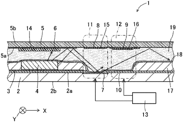
| CPC G02F 1/133512 (2013.01) [G02F 1/1334 (2013.01); G02F 1/1336 (2013.01); G02F 1/133603 (2013.01); G02F 1/133605 (2013.01); G02F 1/13476 (2013.01); G02F 1/136209 (2013.01); H01L 33/60 (2013.01)] | 18 Claims |

|
1. A display device comprising:
a light emitter located on a first light-transmissive substrate;
a second light-transmissive substrate facing the first light-transmissive substrate with the light emitter in between;
a first light-shielding layer located on the first light-transmissive substrate and located away from the light emitter;
a first portion located on the second light-transmissive substrate and facing the first light-shielding layer;
a second light-shielding layer located on the second light-transmissive substrate and located away from the first portion;
a first light output section between the first light-shielding layer and the first portion, the first light output section being switchable between a transmissive state and a scattering state;
a second portion located on the first light-transmissive substrate and facing the second light-shielding layer; and
a second light output section between the second light-shielding layer and the second portion, the second light output section being switchable between the transmissive state and the scattering state.
|