| CPC G02B 6/305 (2013.01) | 20 Claims |

|
1. A method for forming a semiconductor device, comprising:
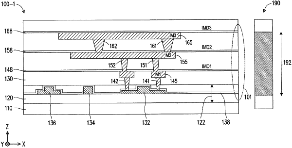
(a) forming an optical waveguide on a silicon-on-insulator (SOI) substrate;
(b) depositing a coupling layer on the optical waveguide and the SOI substrate;
(c) depositing a dielectric layer on the coupling layer;
(d) etching the dielectric layer to form a metal layer in the dielectric layer;
(e) forming an inter-metal dielectric (IMD) layer on the metal layer, wherein the IMD layer serves as an additional coupling layer; and
(f) repeating the above steps (c) to (e) for a predetermined number of times to generate a plurality of coupling layers, wherein:
the plurality of coupling layers include a plurality of coupling pillars disposed at an edge of the semiconductor device,
the plurality of coupling pillars form an edge coupler configured for optically coupling the optical waveguide to an optical fiber placed at the edge of the semiconductor device,
the optical waveguide comprises a plurality of gratings formed using silicon, and
at least two of the plurality of gratings have different shapes from each other.
|