| CPC G01J 1/44 (2013.01) [G01N 21/6408 (2013.01); G01N 21/6458 (2013.01); H04N 25/77 (2023.01); G01J 2001/446 (2013.01); G01J 2001/448 (2013.01); G01N 21/6428 (2013.01); G01N 2021/6439 (2013.01); G06T 7/0012 (2013.01); G06T 2207/10028 (2013.01); G06T 2207/10064 (2013.01); G06T 2207/30204 (2013.01); H04N 25/76 (2023.01)] | 20 Claims |

|
1. A system, comprising:
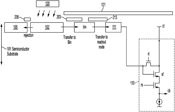
an integrated circuit comprising a pixel, the pixel comprising:
a photodetection region configured to receive incident photons, the photodetection region being configured to produce a plurality of charge carriers in response to the incident photons;
a first charge carrier storage region;
a second charge carrier storage region; and
an electrode located, at least in part, at a boundary of the photodetection region and the first charge carrier storage region to form a potential barrier between the photodetection region and the first charge carrier storage region,
wherein the system comprises a control circuit configured to control the pixel to:
aggregate, in the first charge carrier storage region, first charge carriers at least in part by lowering the potential barrier formed by the electrode to allow charge carrier transfer from the photodetection region to the first charge carrier storage region, the first charge carriers produced by the photodetection region within a first time period with respect to first trigger events;
aggregate, in the first charge carrier storage region, second charge carriers at least in part by lowering the potential barrier formed by the electrode to allow charge carrier transfer from the photodetection region to the first charge carrier storage region, the second charge carriers produced by the photodetection region within a second time period with respect to second trigger events;
read out signals representative of a first quantity of the first charge carriers and a second quantity of the second charge carriers; and
receive, from the first charge carrier storage region, and hold, in the second charge carrier storage region, the first charge carriers to be read out while the first charge carrier storage region receives the second charge carriers.
|