| CPC G01C 3/06 (2013.01) [G01S 7/4914 (2013.01); G01S 7/4915 (2013.01); G01S 17/894 (2020.01); G01S 17/931 (2020.01); H01L 31/0203 (2013.01); H01L 31/02164 (2013.01); H01L 31/0232 (2013.01); H01L 31/107 (2013.01); G01C 3/08 (2013.01)] | 12 Claims |

|
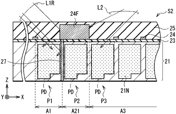
1. A distance measuring device, comprising:
a light-receiving section that includes:
a semiconductor substrate;
a first light-receiving pixel;
a second light-receiving pixel;
a light-shielded pixel that is light-shielded, wherein
each of the first light-receiving pixel, the light-shielded pixel, and the second light-receiving pixel includes a light-receiving element in the semiconductor substrate,
each of the first light-receiving pixel and the second light-receiving pixel is configured to detect first light, and
the first light-receiving pixel, the light-shielded pixel, and the second light-receiving pixel are disposed in a first direction in this order; and
a light-shielding wall in the semiconductor substrate, wherein the light-shielding wall is between the light-receiving element of the first light-receiving pixel and the light-receiving element of the light-shielded pixel; and
a processor configured to measure a distance to a measurement object based on the detected first light.
|