| CPC B81B 7/0051 (2013.01) [B81C 1/00325 (2013.01); B81B 2203/033 (2013.01); B81B 2207/07 (2013.01); B81B 2207/096 (2013.01); B81C 2203/0118 (2013.01)] | 17 Claims |

|
1. A method for producing sensor devices, the method comprising:
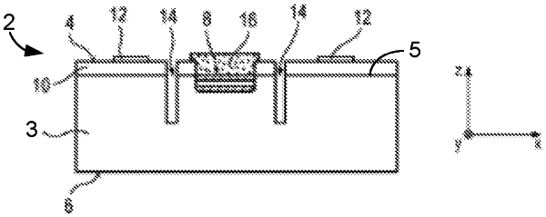
generating a semiconductor wafer having a plurality of sensor chips, wherein a plurality of micro-electromechanical systems (MEMS) structures are arranged at a main surface of the semiconductor wafer, wherein each sensor chip comprises a MEMS structure integrated in the semiconductor wafer at the main surface of the semiconductor wafer, and wherein each MEMS structure resides within a semiconductor material of the semiconductor wafer that is allocated to a respective sensor chip of the plurality of sensor chips;
forming a plurality of trenches that extend from the main surface of the semiconductor wafer into the semiconductor wafer, wherein, one or more trenches of the plurality of trenches laterally surround a respective MEMS structure within the semiconductor material;
forming a plurality of gas-permeable covers over the main surface of the semiconductor wafer, wherein each gas-permeable cover covers a corresponding MEMS structure of the plurality of MEMS structures and forms a cavity above the corresponding MEMS structure such that a plurality of cavities are formed above the plurality of MEMS structures, wherein each cavity is formed between a corresponding MEMS structure and a corresponding gas-permeable cover; and
singulating the semiconductor wafer into a plurality of sensor devices, wherein each sensor device includes a corresponding sensor chip.
|