| CPC H10N 70/801 (2023.02) [H10N 70/011 (2023.02); H10N 70/231 (2023.02)] | 20 Claims |
|
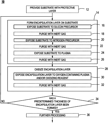
1. A method of forming a stack, the method comprising:
forming an encapsulation layer on the stack on a substrate, the substrate having at least one feature, the encapsulation layer comprising one or more of silicon nitride (SiN) or silicon carbonitride (SiCN); and
oxidizing the encapsulation layer to form a dielectric layer having a dielectric constant in a range of from 4.0 to less than 7.0,
wherein the substrate comprises one or more of a chalcogen, carbon, and a metal and the stack comprises at least one material that is sensitive to air or moisture, and each of the stack and the substrate is substantially undamaged.
|