US 11,800,822 B2
Memory device with composite spacer
Fu-Ting Sung, Taoyuan (TW); Chern-Yow Hsu, Hsinchu County (TW); and Shih-Chang Liu, Kaohsiung (TW)
Assigned to TAIWAN SEMICONDUCTOR MANUFACTURING CO., LTD., Hsinchu (TW)
Filed by TAIWAN SEMICONDUCTOR MANUFACTURING CO., LTD., Hsinchu (TW)
Filed on Jan. 10, 2022, as Appl. No. 17/572,599.
Application 15/783,030 is a division of application No. 14/740,101, filed on Jun. 15, 2015, granted, now 9,806,254, issued on Oct. 31, 2017.
Application 17/572,599 is a continuation of application No. 16/715,868, filed on Dec. 16, 2019, granted, now 11,227,993.
Application 16/715,868 is a continuation of application No. 15/783,030, filed on Oct. 13, 2017, granted, now 10,510,952, issued on Dec. 17, 2019.
Prior Publication US 2022/0131072 A1, Apr. 28, 2022
Int. Cl. H10N 70/20 (2023.01); H10N 50/01 (2023.01); H10N 70/00 (2023.01)
CPC H10N 70/24 (2023.02) [H10N 50/01 (2023.02); H10N 70/011 (2023.02); H10N 70/063 (2023.02); H10N 70/20 (2023.02); H10N 70/801 (2023.02); H10N 70/826 (2023.02)] 20 Claims
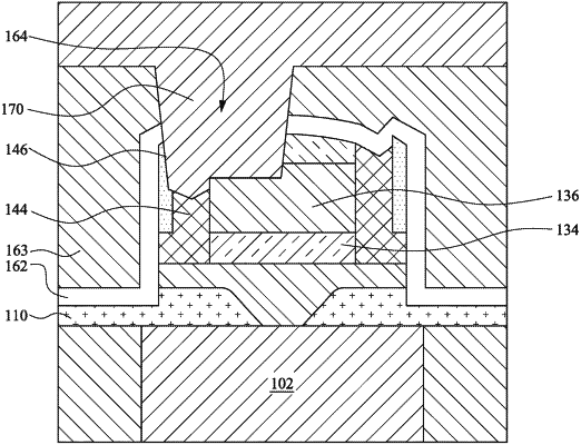
OG exemplary drawing
 
1. A memory device, comprising:
a bottom electrode;
a magnetic tunnel junction (MTJ) structure over the bottom electrode, the bottom electrode having a top surface extending past opposite sidewalls of the MTJ structure;
an inner spacer contacting the top surface of the bottom electrode and one of the opposite sidewalls of the MTJ structure; and
an outer spacer contacting an outer sidewall of the inner spacer, the outer spacer protruding from a top surface of the inner spacer by a step height, wherein the outer spacer has a bottom surface higher than the top surface of the bottom electrode.