| CPC H10N 70/063 (2023.02) [H10B 63/84 (2023.02); H10N 70/043 (2023.02); H10N 70/245 (2023.02); H10N 70/826 (2023.02); H10B 63/20 (2023.02); H10N 70/882 (2023.02)] | 20 Claims |
|
1. A memory device, comprising:
a first access line;
a second access line; and
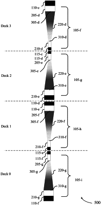
a memory cell coupled with the first access line and the second access line, the memory cell comprising a chalcogenide memory storage element doped with a dopant, a concentration of the dopant in the chalcogenide memory storage element affecting an etching rate of the chalcogenide memory storage element, wherein the chalcogenide memory storage element comprises:
a first portion having a first width and a first doping concentration of the dopant, the first portion etched to the first width based at least in part on the first doping concentration; and
a second portion having a second width and a second doping concentration of the dopant, the second portion etched to the second width based at least in part on the second doping concentration, wherein the first portion and the second portion form a stepped profile of the chalcogenide memory storage element.
|