US 11,800,812 B2
Integrated circuit
Tai-Yen Peng, Hsinchu (TW); Chien-Chung Huang, Taichung (TW); Yu-Shu Chen, Hsinchu (TW); Sin-Yi Yang, Taichung (TW); Chen-Jung Wang, Hsinchu (TW); Han-Ting Lin, Hsinchu (TW); Chih-Yuan Ting, Taipei (TW); Jyu-Horng Shieh, Hsinchu (TW); and Hui-Hsien Wei, Taoyuan (TW)
Assigned to TAIWAN SEMICONDUCTOR MANUFACTURING CO., LTD., Hsinchu (TW)
Filed by TAIWAN SEMICONDUCTOR MANUFACTURING CO., LTD., Hsinchu (TW)
Filed on Mar. 7, 2022, as Appl. No. 17/688,370.
Application 17/688,370 is a division of application No. 16/866,114, filed on May 4, 2020, granted, now 11,271,150.
Application 16/866,114 is a division of application No. 16/194,124, filed on Nov. 16, 2018, granted, now 10,651,373, issued on May 12, 2020.
Claims priority of provisional application 62/737,928, filed on Sep. 28, 2018.
Prior Publication US 2022/0190237 A1, Jun. 16, 2022
Int. Cl. H10B 61/00 (2023.01); H10N 50/01 (2023.01); H10N 50/80 (2023.01)
CPC H10N 50/01 (2023.02) [H10B 61/10 (2023.02); H10B 61/22 (2023.02); H10B 61/00 (2023.02); H10N 50/80 (2023.02)] 20 Claims
OG exemplary drawing
 
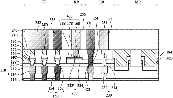
1. An integrated circuit, comprising:
a dielectric layer;
a memory device comprising:
a bottom electrode via in the dielectric layer, wherein the dielectric layer has a first portion extending along sidewalls of the bottom electrode via, a second portion extending laterally from the first portion, and a third portion;
a bottom electrode over the bottom electrode via;
a resistance switching element over the bottom electrode; and
a top electrode over the resistance switching element; and
a resistor over the third portion of the dielectric layer, wherein a thickness of the third portion of the dielectric layer is greater than a thickness of the second portion of the dielectric layer.