| CPC H10B 61/22 (2023.02) [H10N 50/01 (2023.02); H10N 50/80 (2023.02)] | 20 Claims |
|
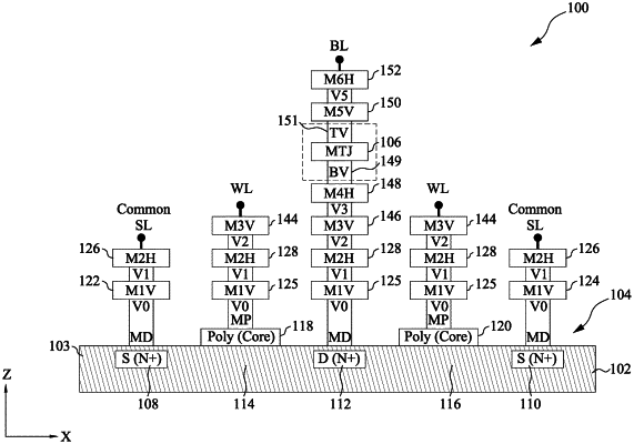
1. An MRAM memory cell, comprising:
a substrate;
a transistor over the substrate and including:
a first source region;
a second source region;
a drain region between the first and second source regions;
at least one first channel region between the drain region and the first source region;
at least one second channel region between the drain region and the second source region;
a first gate structure overlying the at least one first channel region; and
a second gate structure overlying the at least one second channel region;
a magnetic tunnel junction overlying the transistor, wherein the drain region is coupled to the magnetic tunnel junction;
a first metal layer overlying the transistor; and
a second metal layer overlying the first metal layer, wherein the second and first metal layers are configured to couple a common source line signal to the first and second source regions and to first neighboring first and second source regions of a first neighboring transistor of a first neighboring MRAM memory cell; and
a third metal layer overlying the second metal layer, the third metal layer being configured to couple a word line signal to the first and second gate structures.
|