| CPC H10B 12/482 (2023.02) [H01L 21/3086 (2013.01); H01L 21/76224 (2013.01); H10B 12/053 (2023.02); H10B 12/34 (2023.02); H10B 12/485 (2023.02); H10B 12/488 (2023.02)] | 11 Claims |
|
1. A method for forming a memory device, comprising:
providing a substrate;
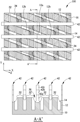
forming an isolation structure in the substrate to define a plurality of active regions in the substrate, the active regions respectively comprising two terminal portions and a central portion between the terminal portions;
forming a plurality of island features on the substrate, wherein in a top view, the island features are separated from each other and each of the island features covers two of the terminals portions respectively belonging to two of the active regions;
performing a first etching process, using the island features as an etching mask to etch the substrate to define a plurality of island structures and a first recessed region between the island structures on the substrate; and
removing the island features to expose the island structures.
|