|
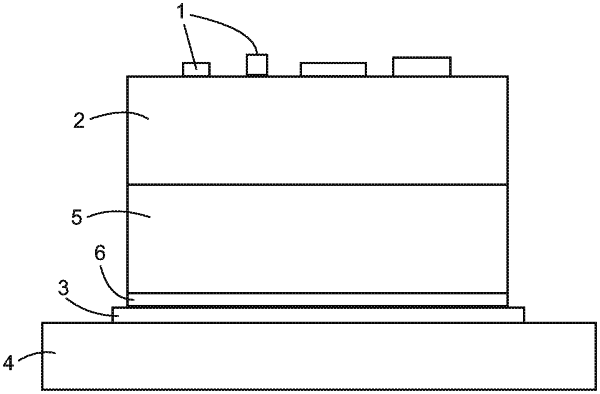
1. A thermalization arrangement at cryogenic temperatures, wherein the arrangement comprises a dielectric substrate layer on which substrate a device/s or component/s are positionable, and a heat sink component attached on another side of the substrate, the arrangement further comprising a conductive layer between the substrate layer and the heat sink component, a joint between the substrate layer and the conductive layer having minimal phonon thermal boundary resistance, and in which energy of conductive layer phonons are arranged to be absorbed by electrons, and another joint between the conductive layer and the heat sink component being electrically conductive, wherein the conductive layer is degenerately doped silicon.
|