| CPC H05K 1/118 (2013.01) [H05K 1/111 (2013.01); H05K 3/361 (2013.01); H05K 2201/09418 (2013.01)] | 10 Claims |
|
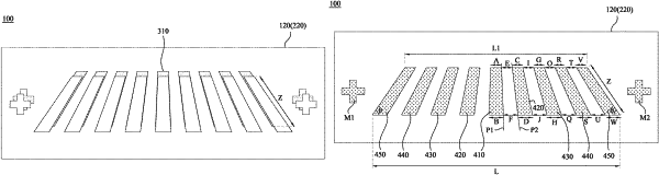
1. A bonding pad structure for an electronic device, comprising:
a substrate, comprising:
a plurality of first pins, disposed on the substrate; and
a flexible printed circuit board, comprising:
a plurality of second pins, disposed on the flexible printed circuit board;
wherein the first pins and the second pins are bonded to each other to define a plurality of bonding pins, and the bonding pins comprise:
at least one central bonding pin, located in a central location of the bonding pins of the electronic device;
at least two first bonding pins, located farthest away from the at least one central bonding pin, wherein the at least two first bonding pins have mirror symmetry with respect to the at least one central bonding pin; and
at least two second bonding pins, located between the at least one central bonding pin and the at least two first bonding pins, wherein the at least two second bonding pins have mirror symmetry with respect to the at least one central bonding pin;
wherein the at least one central bonding pin comprises:
a first end and a second end, wherein a first width of the first end is set to be A, a second width of the second end is set to be B, and A and B satisfy a first relation 0<a/b≤1;
wherein a tilt angle is defined between one of the at least two first bonding pins and one side of the substrate, the tilt angle is set to be θ, and θ satisfies a second relation 0<θ≤90;
wherein a first end of a first pin of the first pins and a first end of a corresponding first pin of the second pins are equal in width;
wherein one of the at least two second bonding pins comprises:
a third end and a fourth end, wherein a third width of the third end is set to be C, a fourth width of the fourth end is set to be D, and C and D satisfy a third relation 0<C/D≤1;
wherein the first width of the first end of the at least one central bonding pin is the same as the third width of the third end of the one of the at least two second bonding pins;
wherein the second width of the second end of the at least one central bonding pin is the same as the fourth width of the fourth end of the one of the at least two second bonding pins;
wherein a first spacing is defined between the first end of the at least one central bonding pin and the third end of the one of the at least two second bonding pins, wherein the first spacing, the first width of the first end, and the third width of the third end are all the same;
wherein a second spacing is defined between the second end of the at least one central bonding pin and the fourth end of the one of the at least two second bonding pins, the second spacing, the second width of the second end, and the fourth width of the fourth end are all the same, and the first spacing is smaller than the second spacing.
|