| CPC H05K 1/0221 (2013.01) [H01L 21/02008 (2013.01); H01L 23/06 (2013.01); H05K 1/0222 (2013.01); H05K 1/0245 (2013.01); H05K 1/115 (2013.01); H05K 3/42 (2013.01)] | 20 Claims |
|
1. A method, comprising:
forming at least one differential coaxial through-via in a dielectric core having a first conducting layer on a first side of said dielectric core and a second conducting layer on a second side of said dielectric core opposite said first side, the dielectric core having a dielectric constant, the forming of the at least one differential coaxial through-via comprising:
forming an annular-shaped outer through-via pattern extending from said first side to said second side;
conductor lining said annular-shaped outer through-via pattern;
filling said annular-shaped outer through-via pattern with a dielectric material or insulative material to complete an outer ground shield enclosure, the outer ground shield enclosure extending from the first side of the dielectric core to the second side of the dielectric core, the outer ground shield enclosure coupled to a ground terminal;
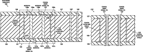
forming through-holes through said dielectric material including first and second inner signal through-hole vias, and
lining said first and second inner signal through-hole vias with a conductive material to form first and second inner signal through-vias that couple from said first conducting layer to said second conducting layer and extend parallel to each other and parallel to the outer ground shield enclosure, each of the first and second inner signal through-vias extending through the dielectric core and having first and second ends terminating at the first and second sides of the dielectric core, the outer ground shield enclosure laterally surrounding a portion of the first inner signal through-via and a portion of the second inner signal through-via;
forming a first contact in the first conducting layer, over the first inner signal through-via, and extending beyond the first inner signal through-via along the first side of the dielectric core;
forming a second contact in the second conducting layer, over the first inner signal through-via and extending beyond the first inner signal through-via along the second side of the dielectric core;
positioning a first side of a first dielectric layer in physical contact with the first side of the dielectric core; and
positioning a first side of a second dielectric layer in physical contact with the second side of the dielectric core,
wherein the outer ground shield enclosure comprises:
an inner face and an outer face opposite of the inner face, the inner face concave and the outer face convex, wherein a first minimum distance between the inner face and the first inner signal through-via and a second minimum distance between the inner face and the second inner signal through-via are each based on the dielectric constant;
a first portion electrically connected to the inner face, extending radially outward from the outer around shield enclosure, and disposed on the first side of the dielectric core; and
a second portion electrically connected to the inner face, extending radially outward from the outer ground shield enclosure, and disposed on the second side of the dielectric core.
|