| CPC H04N 25/70 (2023.01) [G03B 17/02 (2013.01); H01L 27/146 (2013.01); H01L 27/14618 (2013.01); H01L 27/14636 (2013.01); H04N 23/00 (2023.01); H04N 23/54 (2023.01); H04N 23/57 (2023.01); H04N 25/44 (2023.01); H05K 1/185 (2013.01); H05K 3/103 (2013.01); H05K 2201/095 (2013.01); H05K 2201/09118 (2013.01)] | 16 Claims |
|
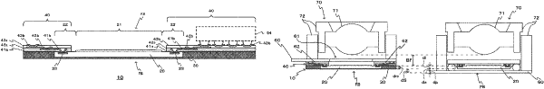
1. An optical device, comprising:
a pixel formation surface;
an imaging element that includes:
a lens;
a pixel region on the pixel formation surface; and
a rewiring region, wherein
the rewiring region is in a first region, of the imaging element, different from the pixel region, and
the rewiring region includes a pad;
a mold part around the imaging element, wherein the mold part is in a second region, of the optical device, different from the pixel formation surface;
a rewiring layer on each of a pixel formation surface side of the imaging element and a pixel formation surface side of the mold part, wherein the rewiring layer is configured to connect an external terminal and the pad; and
a third region on the pixel formation surface side of the mold part, wherein
the third region is for arrangement of a circuit element to be connected to the rewiring layer, and
the external terminal corresponds to a terminal of the circuit element.
|