| CPC H03K 17/0822 (2013.01) [H02H 9/02 (2013.01); H02H 9/041 (2013.01); H02M 3/158 (2013.01); H03K 17/687 (2013.01); H03K 2217/0063 (2013.01)] | 14 Claims |
|
1. A semiconductor device, comprising:
a first power supply terminal to which a first power supply voltage is applied;
a second power supply terminal to which a second power supply voltage lower than the first power supply voltage is applied;
a load terminal to which a load is coupled;
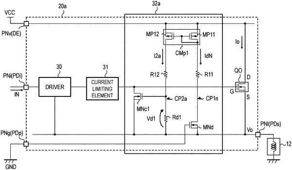
an output transistor which is coupled between the first power supply terminal and the load terminal and is controlled based on a control voltage between a control node thereof and the load terminal;
a driver which controls the control voltage based on a control input signal;
a first current path formed between the first power supply terminal and the load terminal;
a detection transistor which is inserted in the first current path and flows a detection current to the first current path in a period when an output voltage generated at the load terminal is lower than the second power supply voltage;
a current mirror circuit that transfers the detection current flowing through the first current path to a second current path;
a detection resistor element which is inserted in the second current path and converts a current flowing through the second current path to a detection voltage; and
a control transistor which is turned on in a period when the detection voltage converted by the detection resistor element is higher than a predetermined value,
wherein the output transistor is controlled to an off-state in a period when the control transistor is in an on-state.
|