| CPC H03K 17/08122 (2013.01) | 11 Claims |
|
1. A process comprising:
(a) sending a first encoded signal from a modulator, the first encoded signal having a first frequency, and the first encoded signal generated responsive to receiving first data from a first data circuit, wherein the first data circuit includes:
a first sensor having a first sensor output; and
an edge detector having an edge detect input and an edge detect output, wherein the edge detect input is coupled to the first sensor output, and the edge detector is configured to provide the first encoded signal at the edge detect output;
(b) sending a second encoded signal from the modulator, the second encoded signal having a second frequency greater than the first frequency, and the second encoded signal generated responsive to receiving second data from a second sensor; and
(c) sending a third encoded signal from the modulator, the third encoded signal having a third frequency less than the first frequency, and the third encoded signal generated responsive to receiving third data from a third sensor;
wherein the modulator includes:
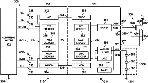
a low voltage stage having a pulse width modulation input, a reset input, a low stage isolation barrier output, a low stage isolation barrier input, and first and second sensor outputs;
an isolation barrier that includes:
a first device having an input and an output, wherein the input is coupled to the low stage isolation barrier output; and
a second device having an input and an output, wherein the output is coupled to the low stage isolation barrier input; and
a high voltage stage having a high stage isolation barrier input, a high stage isolation barrier output, a supply voltage input, a driver output, and first, second and third sensor inputs, wherein the high stage isolation barrier input is coupled to the output of the first device, and the high stage isolation barrier output is coupled to the input of the second device.
|