| CPC H03H 3/02 (2013.01) [H03H 3/04 (2013.01); H03H 9/02102 (2013.01); H03H 9/02149 (2013.01); H03H 9/1007 (2013.01); H03H 9/1057 (2013.01); H03H 9/175 (2013.01); H01L 23/3107 (2013.01); H01L 23/3171 (2013.01); H01L 23/49838 (2013.01); H03H 9/0542 (2013.01); H03H 2003/023 (2013.01); H03H 2003/027 (2013.01); Y10T 29/42 (2015.01); Y10T 29/49171 (2015.01); Y10T 29/49172 (2015.01)] | 20 Claims |
|
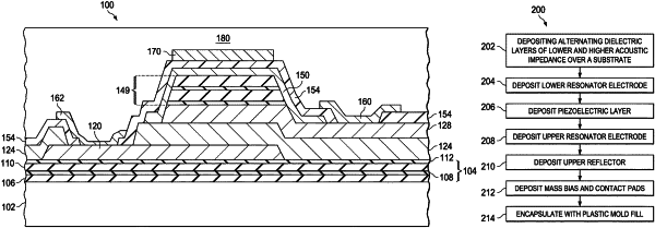
1. A method of forming a resonator, comprising:
forming a bottom dielectric structure over a substrate;
forming a top dielectric structure over the substrate;
forming a piezoelectric layer between the top and bottom dielectric structures;
forming a bottom electrode between the piezoelectric layer and the bottom dielectric structure;
forming a top electrode between the piezoelectric layer and the top dielectric structure;
forming a metal layer over the top dielectric structure; and
patterning the metal layer thereby forming a first contact pad making electrical contact to the top electrode, a second contact pad making electrical contact with the bottom electrode, and a mass bias located over the top dielectric structure.
|