| CPC H02M 3/003 (2021.05) [H05K 1/181 (2013.01); H05K 3/303 (2013.01); H05K 2201/10325 (2013.01); H05K 2201/10719 (2013.01)] | 13 Claims |
|
1. A package structure, comprising:
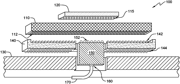
an interconnect component located between a package substrate and a motherboard, wherein a top surface of the interconnect component is connected to a bottom surface of the package substrate, and a bottom surface of the interconnect component is connected to a top surface of the motherboard;
a DC-DC power converter attached to the bottom surface of the package substrate, wherein a plurality of output terminals of the DC-DC power converter are electromechanically connected to the bottom surface of the package substrate via a plurality of solder balls forming a ball grid array (BGA), and wherein the DC-DC power converter is located at least within an open area of the interconnect component located between the package substrate and the motherboard; and
an electrical input cable that provides input power and current to the DC-DC power converter, wherein the electrical input cable is routed laterally through the interconnect component located between the package substrate and the motherboard.
|