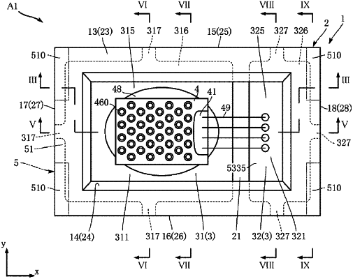
| CPC H01S 5/02257 (2021.01) [H01S 5/02216 (2013.01); H01S 5/02315 (2021.01); H01L 2224/32245 (2013.01); H01L 2224/48227 (2013.01); H01L 2224/48471 (2013.01); H01L 2224/49175 (2013.01); H01L 2924/16195 (2013.01); H01S 5/0237 (2021.01); H01S 5/02335 (2021.01); H01S 5/02345 (2021.01); H01S 5/18313 (2013.01); H01S 5/18347 (2013.01); H01S 5/3432 (2013.01); H01S 5/34353 (2013.01); H01S 5/423 (2013.01)] | 19 Claims |

|
1. A semiconductor light-emitting device, comprising:
a semiconductor light-emitting element;
a support including a base and a conductive part and configured to support the semiconductor light-emitting element; and
a cover configured to overlap the semiconductor light-emitting element as viewed in a first direction, and to transmit light from the semiconductor light-emitting element,
wherein the cover includes a base layer having a front surface and a rear surface which transmit the light from the semiconductor light-emitting element and face opposite sides to each other in the first direction,
wherein the rear surface faces the semiconductor light-emitting element,
wherein the base layer includes a plurality of undulation parts that faces the support,
wherein the undulation parts are more uneven than the rear surface in a first sectional view taken along a second direction perpendicular to the first direction,
wherein the support includes:
a first surface on which the semiconductor light-emitting element is arranged;
a second surface configured to support the base layer, an entire area of the second surface being bonded to the undulation parts via a bonding material to bond the base layer to the support; and
a third surface that is inclined with respect to the first surface, connected to the first surface and the second surface, and formed to surround the first surface as viewed in the first direction,
wherein the undulation parts are formed to extend inward more than the second surface as viewed in the first direction, and overlap the third surface as viewed in the first direction,
wherein the bonding material between the base layer and the second surface fills the undulation parts, and is in contact with a part of the third surface, and
wherein at an edge portion of the semiconductor light-emitting device in the second direction, a central portion of the base layer is thicker than a peripheral portion of the base layer in a second sectional view taken along a third direction perpendicular to the first direction and the second direction.
|