| CPC H01Q 1/40 (2013.01) [G06F 1/1633 (2013.01); H05K 5/0217 (2013.01); H05K 5/0247 (2013.01); H01Q 1/22 (2013.01)] | 7 Claims |
|
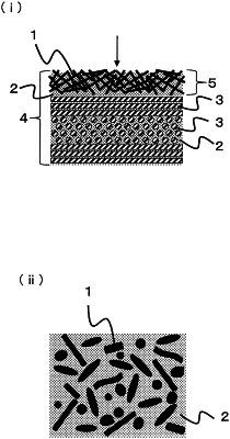
1. An electronic device housing comprising a fiber reinforcing member (a) and a fiber reinforcing member (b), wherein
the fiber reinforcing member (a) contains a thermoplastic resin (a1) and discontinuous fibers (a2),
the fiber reinforcing member (b) contains a thermosetting resin (b1) and continuous fibers (b2) that are not electrically conductive, and does not contain any fibers that are electrically conductive,
a projected area of the fiber reinforcing member (a) accounts for 80% or more and 95% or less of the total projected area, which accounts for 100%, of the electronic device housing projected onto a plane, and
the thermoplastic resin (a1) has a property (i) and/or (ii) given below:
(i) a melting point of more than 265° C., and
(ii) a water absorption rate of 0.4% or less.
|