| CPC H01L 31/107 (2013.01) [G02B 3/00 (2013.01); H01L 27/14 (2013.01); H01L 27/146 (2013.01); H01L 27/14603 (2013.01); H01L 27/14627 (2013.01); H01L 27/14629 (2013.01); H01L 27/14636 (2013.01); H01L 27/14643 (2013.01); H01L 31/02327 (2013.01); H01L 31/022408 (2013.01); H04N 25/134 (2023.01); H04N 25/62 (2023.01); H04N 25/70 (2023.01); H04N 25/76 (2023.01); G02B 3/0056 (2013.01)] | 10 Claims |
|
1. A solid-state imaging element, comprising:
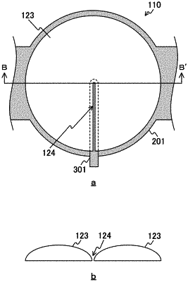
a photodiode that includes a light receiving surface and an electrode placed on the light receiving surface, and that outputs an electrical signal in accordance with light incident on the light receiving surface in a state where a voltage exceeding a breakdown voltage is applied to the electrode;
a signal line, wherein the signal line is a wiring that extends across a portion of the light receiving surface of the photodiode and is electrically connected to the electrode; and
a light collecting section that causes light from a subject to be collected in the light receiving surface other than a region where the electrode is placed,
wherein the light collecting section includes a microlens,
wherein the microlens has a cut in a bottom portion of the microlens, and
wherein the cut is placed along the signal line.
|