| CPC H01L 29/78391 (2014.09) [H01L 29/40111 (2019.08); H01L 29/516 (2013.01)] | 20 Claims |
|
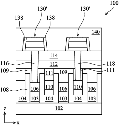
1. A device, comprising:
a substrate;
gate stacks and source/drain (S/D) features over the substrate;
S/D contacts over the S/D features;
one or more dielectric layers over the gate stacks and the S/D contacts;
a via penetrating the one or more dielectric layers and electrically contacting one of the gate stacks and the S/D contacts, wherein the via is above the one of the gate stacks and S/D contacts; and
a ferroelectric (FE) stack over the via and directly contacting the via, wherein the FE stack includes an FE feature and a top electrode over the FE feature.
|