| CPC H01L 29/7397 (2013.01) [H01L 27/0635 (2013.01); H01L 29/66348 (2013.01)] | 11 Claims |
|
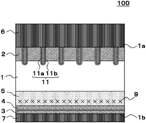
1. A semiconductor device comprising:
a drift layer of a first conduction type provided in a semiconductor substrate having a first principal plane and a second principal plane opposed to the first principal plane;
a first semiconductor layer of a second conduction type provided between the first principal plane of the semiconductor substrate and the drift layer and having an impurity concentration higher than an impurity concentration of the drift layer;
a first buffer layer of the first conduction type provided between the second principal plane of the semiconductor substrate and the drift layer and having hydrogen-induced donors with an impurity concentration higher than the impurity concentration of the drift layer; and
a second semiconductor layer of the first conduction type or the second conduction type provided between the second principal plane of the semiconductor substrate and the first buffer layer and having an impurity concentration higher than the impurity concentration of the drift layer,
wherein the first buffer layer includes a complex defect of interstice carbon and interstice oxygen having a density decreasing from a second principal plane side toward a first principal plane side.
|