| CPC H01L 29/6681 (2013.01) [H01L 21/823431 (2013.01); H01L 29/0649 (2013.01); H01L 29/0669 (2013.01)] | 20 Claims |
|
1. A semiconductor structure comprising:
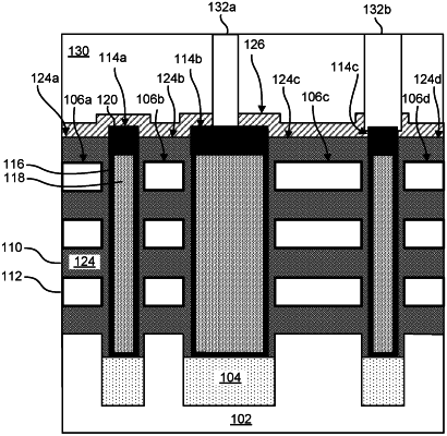
a plurality of fin structures extending along a first direction over a substrate;
a plurality of gate structure segments positioned along a line extending in a second direction, the second direction being orthogonal to the first direction, wherein the gate structure segments are separated by dummy fin structures, wherein the dummy fin structures include a first dummy fin structure having a first sidewall, a second sidewall that opposes the first sidewall and a topmost surface extending from the first sidewall to the second sidewall;
a conductive layer disposed over both the gate structure segments and the dummy fin structures to electrically connect at least some of the gate structure segments; and
a cut feature aligned with one of the dummy fin structures and positioned to electrically isolate gate structure segments on both sides of the one of the dummy fin structures, wherein the cut feature physically contacts the first sidewall, the second sidewall and the topmost surface of the first dummy fin structure.
|