| CPC H01L 29/66795 (2013.01) [H01L 21/0337 (2013.01); H01L 21/324 (2013.01); H01L 21/762 (2013.01); H01L 21/76832 (2013.01); H01L 21/823807 (2013.01); H01L 21/823821 (2013.01); H01L 21/823828 (2013.01); H01L 21/823878 (2013.01); H01L 27/0922 (2013.01); H01L 29/0649 (2013.01); H01L 29/66545 (2013.01); H01L 29/785 (2013.01)] | 20 Claims |

|
1. A method, comprising:
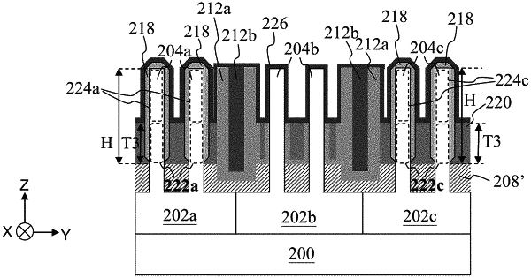
forming a fin structure extending above a dielectric isolation structure disposed over a substrate, the dielectric isolation structure laterally surrounding a bottom portion of the fin structure;
forming a semiconductor liner layer including a dopant over the fin structure;
forming a first capping layer to physically contact a bottom portion of the semiconductor liner layer and the dielectric isolation structure, the bottom portion of the semiconductor liner layer laterally surrounding a lower portion of the fin structure;
forming a second capping layer to physically contact an upper portion of the semiconductor liner layer, the upper portion of the semiconductor liner layer laterally surrounding an upper portion of the fin structure; and
annealing the fin structure having the semiconductor liner layer, the first capping layer, and the second capping layer thereon, the annealing causing the dopant of the semiconductor liner layer to diffuse into the fin structure, wherein an average dopant concentration in a lower portion of the fin structure is different from an average dopant concentration in an upper portion of the channel region.
|