| CPC H01L 29/66757 (2013.01) [H01L 21/02488 (2013.01); H01L 21/02532 (2013.01)] | 18 Claims |
|
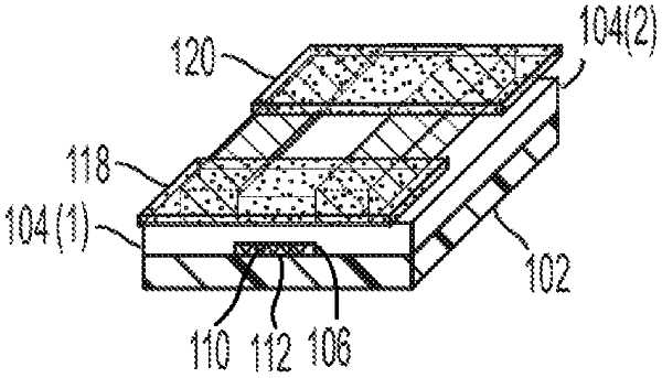
1. A semiconductor device comprising:
a substrate layer;
a first amorphous layer deposited on the substrate layer;
a semiconductor layer deposited on the first amorphous layer, wherein the semiconductor layer does not contact the substrate layer;
a channel formed into the semiconductor layer and into the first amorphous layer;
a second amorphous layer deposited in the channel; and
a semiconductor defect region disposed between the substrate layer and the second amorphous layer.
|