US 11,799,014 B2
Gate structure and methods thereof
Anhao Cheng, Taichung (TW); and Fang-Ting Kuo, Hsinchu County (TW)
Assigned to TAIWAN SEMICONDUCTOR MANUFACTURING CO., LTD., Hsinchu (TW)
Filed by Taiwan Semiconductor Manufacturing Co., Ltd., Hsinchu (TW)
Filed on Jan. 14, 2022, as Appl. No. 17/576,727.
Application 17/576,727 is a division of application No. 16/587,003, filed on Sep. 29, 2019, granted, now 11,227,935.
Application 16/587,003 is a division of application No. 15/884,903, filed on Jan. 31, 2018, granted, now 10,431,664, issued on Oct. 1, 2019.
Claims priority of provisional application 62/527,665, filed on Jun. 30, 2017.
Prior Publication US 2022/0140109 A1, May 5, 2022
This patent is subject to a terminal disclaimer.
Int. Cl. H01L 29/80 (2006.01); H01L 31/112 (2006.01); H01L 29/66 (2006.01); H01L 21/8234 (2006.01); H01L 21/8238 (2006.01); H01L 27/092 (2006.01); H01L 49/02 (2006.01); H03K 19/0185 (2006.01)
CPC H01L 29/66484 (2013.01) [H01L 21/823462 (2013.01); H01L 21/823481 (2013.01); H01L 21/823814 (2013.01); H01L 21/823857 (2013.01); H01L 27/0922 (2013.01); H01L 28/40 (2013.01); H01L 29/66492 (2013.01); H03K 19/018521 (2013.01); H01L 21/823878 (2013.01)] 20 Claims
OG exemplary drawing
 
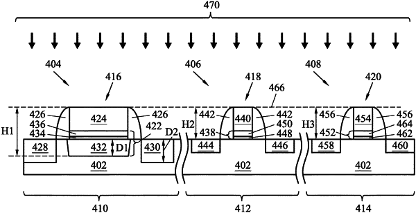
1. A semiconductor device, comprising:
a trench including a first layer of a gate oxide of the semiconductor device disposed therein, the trench disposed in a region of a substrate that is free of a shallow trench isolation feature;
a second layer of the gate oxide of the semiconductor device disposed over the first layer of the gate oxide and outside the trench; and
a source region and a drain region disposed on either side of the trench;
wherein the trench has a first depth, and wherein the source region and the drain region extend into the substrate a second depth greater than the first depth.