| CPC H01L 29/4238 (2013.01) [H01L 27/088 (2013.01); H01L 29/402 (2013.01)] | 20 Claims |
|
1. A semiconductor device comprising:
a first doped region in a substrate, wherein the first doped region has a first dopant type;
a second doped region in the substrate, wherein the second doped region has a second dopant type opposite the first dopant type;
an isolation structure between the first doped region and the second doped region;
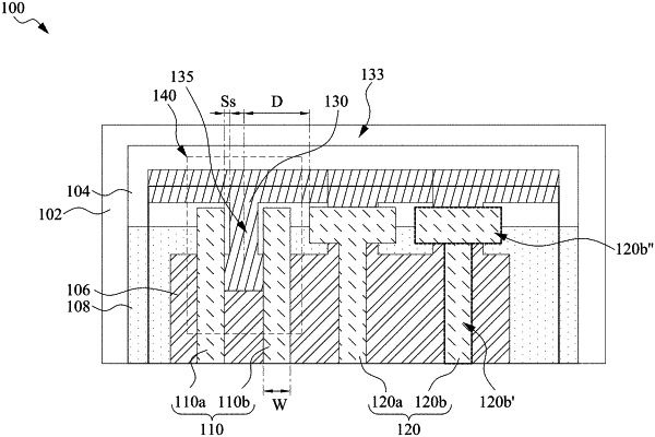
a silicide structure on the substrate, wherein the silicide structure comprises a main body and a silicide extension, and the main body is integral with the silicide extension; and
a plurality of first gate structures on the substrate, wherein each of the plurality of first gate structures continuously extending over the first doped region and the second doped region, a space between adjacent gate structures of the plurality of first gate structures comprises a first area and a second area, the silicide extension extends into the first area, the first doped region is in the substrate below the first area, and the second doped region is in the substrate below the second area.
|