| CPC H01L 29/42368 (2013.01) [H01L 21/76224 (2013.01); H01L 21/823462 (2013.01); H01L 29/401 (2013.01); H01L 29/4236 (2013.01); H01L 29/7813 (2013.01); H01L 29/7825 (2013.01); H01L 29/7834 (2013.01)] | 20 Claims |
|
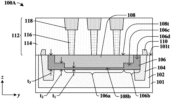
1. A semiconductor device comprising:
a first doped region arranged within a semiconductor substrate, the first doped region having a first doping conductivity;
a second doped region and a third doped region arranged within the semiconductor substrate on opposite sides of the first doped region, the second doped region and the third doped region having a second doping conductivity opposite the first doping conductivity;
a gate electrode arranged over the first doped region, the gate electrode comprising a bottom surface arranged below a topmost surface of the semiconductor substrate; and
a gate dielectric structure separating the gate electrode from the first doped region, wherein the gate dielectric structure comprises a central portion having a first thickness and a corner portion having a second thickness, and wherein the second thickness is at least two times greater than the first thickness; and
a trench isolation structure laterally surrounding the first doped region, the second doped region, and the third doped region, wherein the bottom surface of the gate electrode is below an upper surface of the trench isolation structure.
|