| CPC H01L 29/42364 (2013.01) [H01L 21/265 (2013.01); H01L 21/823468 (2013.01); H01L 29/0611 (2013.01)] | 20 Claims |
|
1. A method for manufacturing a semiconductor device, the method comprising:
depositing a first oxide layer on a first portion, a second portion, and a third portion of a substrate, wherein the first oxide layer is a sacrificial oxide layer for the first portion and the second portion of the substrate;
depositing a first photoresist layer on the first oxide layer deposited on the third portion of the substrate;
removing the first oxide layer from the first portion and the second portion of the substrate;
removing the first photoresist layer from the first oxide layer deposited on the third portion of the substrate;
depositing a second oxide layer on the first portion and the second portion of the substrate and on the first oxide layer deposited on the third portion of the substrate, wherein the first oxide layer and the second oxide layer on the third portion of the substrate define a modified first oxide layer on the third portion of the substrate;
depositing a second photoresist layer on the modified first oxide layer and on the second oxide layer deposited on the second portion of the substrate;
removing the second oxide layer deposited on the first portion of the substrate;
depositing a third oxide layer on the first portion of the substrate after removing the second oxide layer deposited on the first portion of the substrate;
removing the second photoresist layer after depositing the third oxide layer on the first portion of the substrate;
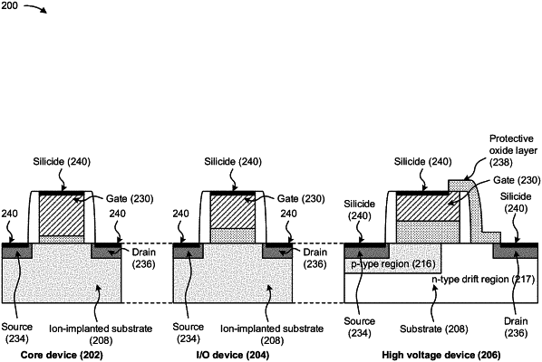
providing a first device on the third oxide layer deposited on the first portion of the substrate;
providing a second device on the second oxide layer deposited on the second portion of the substrate; and
providing a third device on the modified first oxide layer deposited on the third portion of the substrate.
|