| CPC H01L 29/41725 (2013.01) [H01L 21/486 (2013.01); H01L 23/5226 (2013.01)] | 20 Claims |
|
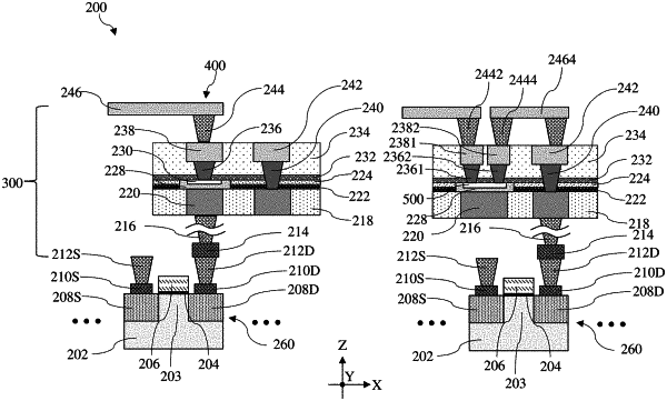
1. A semiconductor structure, comprising:
a transistor; and
an interconnect structure disposed over the transistor, wherein the interconnect structure comprises:
a first dielectric layer,
a first conductive feature in the first dielectric layer,
a first etch stop layer (ESL) disposed on a top surface of the first dielectric layer,
a dielectric feature disposed in the first ESL and in contact with a top surface of the first conductive feature and the top surface of the first dielectric layer,
an electrode disposed over the dielectric feature such that the electrode is vertically spaced apart from the top surface of the first conductive feature by the dielectric feature, and
a second ESL disposed on and in contact with top surfaces of the dielectric feature and the electrode.
|