US 11,798,999 B2
Methods for forming a metal silicate film on a substrate in a reaction chamber and related semiconductor device structures
Fu Tang, Gilbert, AZ (US); Peng-Fu Hsu, Scottsdale, AZ (US); Michael Eugene Givens, Phoenix, AZ (US); and Qi Xie, Wilsele (BE)
Assigned to ASM IP Holding B.V., Almere (NL)
Filed by ASM IP Holding B.V., Almere (NL)
Filed on Jul. 26, 2022, as Appl. No. 17/873,885.
Application 17/026,510 is a division of application No. 16/194,041, filed on Nov. 16, 2018, granted, now 10,818,758, issued on Oct. 27, 2020.
Application 17/873,885 is a continuation of application No. 17/026,510, filed on Sep. 21, 2020, granted, now 11,411,088.
Prior Publication US 2022/0367647 A1, Nov. 17, 2022
This patent is subject to a terminal disclaimer.
Int. Cl. H01L 29/40 (2006.01); H01L 21/02 (2006.01); H01L 21/28 (2006.01); H01L 29/66 (2006.01); C23C 16/40 (2006.01); H01L 29/51 (2006.01); H01L 29/78 (2006.01); H01L 29/161 (2006.01)
CPC H01L 29/408 (2013.01) [C23C 16/401 (2013.01); C23C 16/403 (2013.01); H01L 21/022 (2013.01); H01L 21/0228 (2013.01); H01L 21/02145 (2013.01); H01L 21/02205 (2013.01); H01L 21/28158 (2013.01); H01L 29/161 (2013.01); H01L 29/513 (2013.01); H01L 29/517 (2013.01); H01L 29/66477 (2013.01); H01L 29/78 (2013.01)] 20 Claims
OG exemplary drawing
 
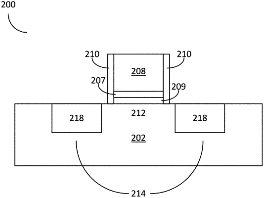
1. A semiconductor device structure comprising:
a silicon germanium channel region;
an interface layer comprising a metal silicate film disposed on the silicon germanium channel region, wherein the metal silicate film comprises a halide level of less than about 0.2 atomic-%; and
a high-k dielectric material disposed on the interface layer.