| CPC H01L 29/404 (2013.01) | 6 Claims |
|
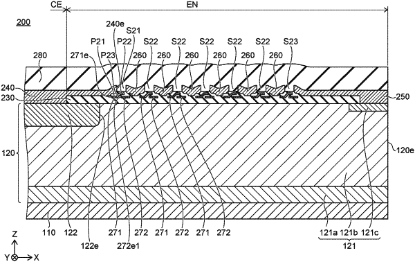
1. A semiconductor device,
a cell region and a termination region being set in the device,
the termination region surrounding the cell region,
the device comprising:
a first electrode;
a semiconductor part located on the first electrode;
an insulating film located on the semiconductor part in the termination region;
a plurality of second electrodes located on the insulating film and arranged in a first direction, the first direction being from a center of the semiconductor part toward an outer perimeter of the semiconductor part when viewed from above, the plurality of second electrodes being separated from each other;
a first floating electrode located in the insulating film, the first floating electrode overlapping a gap between a pair of adjacent second electrodes among the plurality of second electrodes when viewed from above, the first floating electrode facing one of the pair of second electrodes via the insulating film; and
a second floating electrode located in the insulating film, the second floating electrode being separated from the first floating electrode, the second floating electrode overlapping the first floating electrode in the gap when viewed from above, a portion of the second floating electrode overlapping the first floating electrode and being positioned below a portion of the first floating electrode overlapping the gap, the second floating electrode facing the other of the pair of second electrodes via the insulating film.
|