| CPC H01L 29/401 (2013.01) [H01L 21/283 (2013.01); H01L 21/32135 (2013.01); H01L 29/4175 (2013.01); H01L 29/66795 (2013.01); H01L 29/78696 (2013.01)] | 20 Claims |
|
1. A method, comprising:
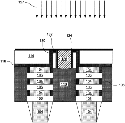
receiving a workpiece comprising:
a substrate,
a first source/drain structure and a second source/drain structure over the substrate,
a plurality of nanostructures extending between and in contact with the first source/drain structure and the second source/drain structure,
a gate structure wrapping around each of the plurality of nanostructures, and
a dummy contact structure embedded in the substrate and disposed under the second source/drain structure;
flipping the workpiece upside down;
selectively removing the substrate without substantially damaging the dummy contact structure;
depositing a first dielectric layer over back surfaces of the gate structure and the first source/drain structure as well as along sidewalls of the dummy contact structure;
depositing a backside dielectric layer over the first dielectric layer;
after the depositing of the backside dielectric layer, selectively removing the dummy contact structure to form an opening that exposes the second source/drain structure;
forming a dummy layer along sidewalls of the opening;
forming a second dielectric layer along sidewalls of the dummy layer in the opening;
after the forming of the second dielectric layer, forming a metal plug in the opening such that the metal plug is spaced apart from the backside dielectric layer by the first dielectric layer, the dummy layer and the second dielectric layer; and
selectively removing the dummy layer to form a gap between the first dielectric layer and the second dielectric layer.
|