| CPC H01L 27/1463 (2013.01) [H01L 31/028 (2013.01); H01L 31/02161 (2013.01)] | 20 Claims |
|
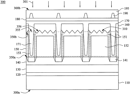
1. A semiconductor device, comprising:
a device layer having a plurality of devices formed therein;
a semiconductor layer on the device layer, wherein:
the semiconductor layer comprises a plurality of isolation regions and a plurality of pixel regions,
each of the plurality of isolation regions comprises a trench isolation and an implanted well surrounding the trench isolation,
the trench isolation comprises a dielectric material,
the implanted well comprises a first semiconductor material, and
the plurality of pixel regions comprises a second semiconductor material that is different from the first semiconductor material; and
an insulation layer on the semiconductor layer,
wherein the insulation layer comprises silicon oxide to serve as a passivation layer for the semiconductor layer, and
wherein the plurality of devices are located entirely below a respective one of the plurality of isolation regions and positioned entirely outside the plurality of pixel regions.
|