| CPC H01L 27/14627 (2013.01) [H01L 23/31 (2013.01); H01L 24/14 (2013.01); H04N 23/55 (2023.01)] | 11 Claims |
|
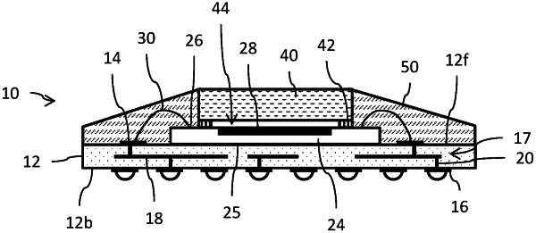
1. An integrated circuit package, comprising:
a support substrate having a front side and a back side;
an optical integrated circuit die having a back side mounted to the front side of the support substrate and having a front side with an optical sensing circuit;
a glass optical element die having a back side mounted to the front side of the optical integrated circuit die over the optical sensing circuit;
a film layer of transparent adhesive positioned between the glass optical element and the optical integrated circuit die, wherein said film layer extends to cover the optical sensing circuit and a portion of the front side of the optical integrated circuit die peripherally surrounding the optical sensing circuit; and
an encapsulation material body which encapsulates the glass optical element die and the optical integrated circuit die.
|