| CPC H01L 27/14607 (2013.01) [H01L 27/1461 (2013.01); H01L 27/1463 (2013.01); H01L 27/1464 (2013.01); H01L 27/14605 (2013.01); H01L 27/14609 (2013.01); H01L 27/14614 (2013.01); H01L 27/14616 (2013.01); H01L 27/14623 (2013.01); H01L 27/14627 (2013.01); H01L 27/14638 (2013.01); H01L 27/14641 (2013.01); H04N 25/585 (2023.01); H04N 25/621 (2023.01); H04N 25/70 (2023.01); H01L 27/14645 (2013.01)] | 2 Claims |
|
1. A solid-state imaging device, comprising:
a pixel array unit which comprises a plurality of pixels, wherein
each pixel of the plurality of pixels includes:
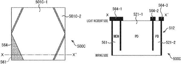
a first photoelectric conversion unit; and
a second photoelectric conversion unit having lower sensitivity than the first photoelectric conversion unit,
the second photoelectric conversion unit is in an outer periphery of the first photoelectric conversion unit,
the second photoelectric conversion unit is in a point-symmetrical region with respect to a center of the first photoelectric conversion unit as a symmetrical point,
a light incident side of a partial region of the second photoelectric conversion unit is shielded from light incident on the light incident side, and
the partial region is used as a memory unit to hold a charge.
|