| CPC H01L 27/092 (2013.01) [H01L 21/02636 (2013.01); H01L 21/30625 (2013.01); H01L 21/823807 (2013.01); H01L 29/0673 (2013.01); H01L 29/0676 (2013.01); H01L 29/1033 (2013.01); H01L 29/16 (2013.01); H01L 29/42392 (2013.01)] | 20 Claims |
|
1. A semiconductor structure, comprising:
a substrate;
a semiconductor layer formed over the substrate;
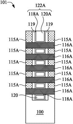
a first channel layer and a second channel layer vertically stacked over the semiconductor layer;
a first insulating structure interposing the first channel layer and the semiconductor layer;
a second insulating structure interposing the first channel layer and the second channel layer;
a gate stack abutting the first channel layer and the second channel layer, wherein the gate stack comprises:
a first portion vertically sandwiched between the first channel layer and the semiconductor layer; and
a second portion vertically sandwiched between the first channel layer and the second channel layer,
wherein a first distance between two opposite edges of the first portion of the gate stack is different from a second distance between two opposite edges of the second portion of the gate stack; and
a source/drain region having a first region attached to the first insulating structure and a second region attached to the second insulating structure, wherein a third distance between two opposite edges of the first region is different from a fourth distance between two opposite edges of the second region.
|