| CPC H01L 27/0886 (2013.01) [H01L 29/0653 (2013.01); H01L 29/0665 (2013.01); H01L 29/16 (2013.01); H01L 29/41791 (2013.01); H01L 29/66795 (2013.01); H01L 29/785 (2013.01); H01L 2029/7858 (2013.01)] | 20 Claims |
|
1. A semiconductor structure comprising:
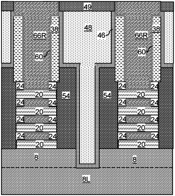
a first gate-all-around field effect transistor located over a substrate and comprising:
at least one silicon portion comprising a middle portion, a first end and a second end;
a first gate structure including a first gate dielectric layer and a first gate electrode and surrounding each middle portion of the at least one silicon portion;
a first source region located on a first end of the at least one silicon portion; and
a first drain region located on a second end of the at least one silicon portion; and
a second gate-all-around field effect transistor located over the substrate, laterally spaced from the first gate-all-around field effect transistor, and comprising:
at least one silicon-germanium portion;
a second gate structure including a second gate dielectric layer and a second gate electrode and surrounding each middle portion of the at least one silicon-germanium portion;
a second source region located on a first end of the at least one silicon-germanium portion; and
a second drain region located on a second end of the at least one silicon-germanium portion,
wherein:
each of the at least one silicon portion and each of the at least one silicon-germanium portion is single crystalline; and
each crystallographic orientation having a same Miller index is orientated along a same direction as the at least one silicon portion and the at least one silicon-germanium portion.
|