| CPC H01L 27/0886 (2013.01) [H01L 21/30608 (2013.01); H01L 21/823418 (2013.01); H01L 21/823431 (2013.01); H01L 29/0843 (2013.01); H01L 29/66795 (2013.01); H01L 29/7851 (2013.01)] | 20 Claims |
|
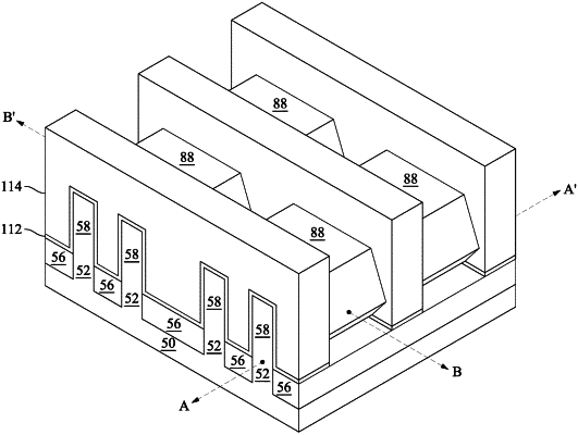
1. A method comprising:
depositing a protective layer on a source/drain region and a gate mask, the gate mask disposed on a gate structure, the gate structure disposed on a channel region of a substrate, the channel region adjoining the source/drain region;
etching an opening through the protective layer, the opening exposing the source/drain region;
depositing a metal in the opening and on the protective layer;
annealing the metal to form a metal-semiconductor alloy region on the source/drain region; and
removing residue of the metal from the opening with a cleaning process, the protective layer covering the gate mask during the cleaning process.
|