| CPC H01L 27/0886 (2013.01) [H01L 21/0217 (2013.01); H01L 21/0223 (2013.01); H01L 21/02255 (2013.01); H01L 21/823431 (2013.01); H01L 21/823437 (2013.01); H01L 21/823481 (2013.01); H01L 21/823821 (2013.01); H01L 27/0924 (2013.01); H01L 29/0649 (2013.01); H01L 29/42376 (2013.01); H01L 29/66545 (2013.01); H01L 29/66553 (2013.01); H01L 21/823828 (2013.01); H01L 21/823878 (2013.01)] | 20 Claims |
|
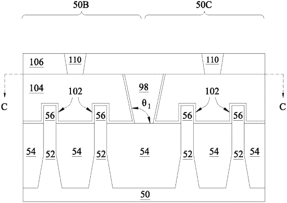
1. A method comprising:
forming a first fin and a second fin extending from a substrate;
forming a dummy gate dielectric on the first fin and the second fin;
forming a dummy gate electrode on the dummy gate dielectric;
patterning an opening in the dummy gate electrode and the dummy gate dielectric, the opening disposed between the first fin and the second fin;
oxidizing sidewalls of the dummy gate electrode to form sacrificial oxides in the opening;
forming a first isolation region between the sacrificial oxides in the opening;
removing the dummy gate electrode with a first etch; and
after removing the dummy gate electrode, removing the dummy gate dielectric and the sacrificial oxides with a second etch, the second etch being selective to materials of the dummy gate dielectric and the sacrificial oxides.
|