| CPC H01L 27/0886 (2013.01) [H01L 21/28525 (2013.01); H01L 21/76897 (2013.01); H01L 21/823431 (2013.01); H01L 21/823475 (2013.01); H01L 21/823481 (2013.01); H01L 29/0847 (2013.01); H01L 29/165 (2013.01); H01L 29/41791 (2013.01); H01L 29/66545 (2013.01); H01L 29/66795 (2013.01); H01L 21/28518 (2013.01); H01L 21/76831 (2013.01); H01L 21/823425 (2013.01); H01L 29/495 (2013.01); H01L 29/4958 (2013.01); H01L 29/4966 (2013.01); H01L 29/4975 (2013.01); H01L 29/665 (2013.01); H01L 29/7853 (2013.01)] | 20 Claims |
|
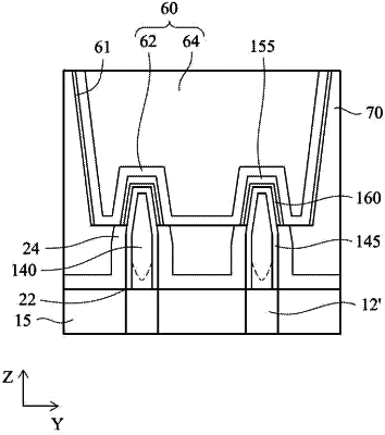
1. A semiconductor device, comprising:
a first source/drain epitaxial layer disposed at a source/drain region of a first fin structure;
a second source/drain epitaxial layer disposed at a source/drain region of a second fin structure;
an etch-stop layer covering part of the first and second source/drain epitaxial layers; and
a third source/drain epitaxial layer disposed on the first and second epitaxial layers and disposed on an upper portion of the etch-stop layer disposed between the first source/drain epitaxial layer and the second source/drain epitaxial layer.
|