| CPC H01L 25/18 (2013.01) [H01L 23/3107 (2013.01); H01L 24/08 (2013.01); H01L 24/32 (2013.01); H01L 2224/08145 (2013.01); H01L 2224/32145 (2013.01)] | 20 Claims |
|
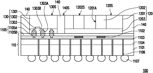
1. A semiconductor package, comprising:
a first die comprising a first substrate and an optical coupler formed on the first substrate;
a second die disposed on the first die and comprising a second substrate and a transparent portion, the transparent portion overlapping the optical coupler; and
a transparent encapsulation material disposed on the first die and laterally encapsulating the second die, the transparent encapsulation material comprising an interface with the second substrate, wherein the transparent portion is spaced apart from the transparent encapsulation material by the second substrate.
|