| CPC H01L 25/0657 (2013.01) [H01L 23/49816 (2013.01); H01L 23/49833 (2013.01); H01L 2225/0651 (2013.01); H01L 2225/06506 (2013.01); H01L 2225/06562 (2013.01)] | 20 Claims |
|
1. An apparatus, comprising:
an integrated circuit die (ICD) substrate having a top surface and a bottom surface, the top surface including a plurality of die contact pads;
a plurality of solder balls at least partially embedded in the bottom surface of the ICD substrate, wherein one or more of the solder balls is in electrical communication with one or more of the die contact pads;
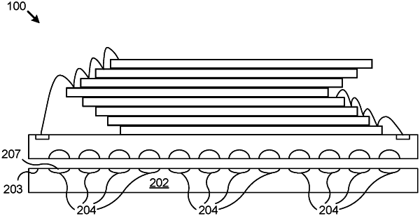
one or more integrated circuit dies attached to the top surface of the ICD substrate and in electrical communication with the die contact pads of the ICD substrate, the one or more integrated circuit dies comprises a plurality of dies that are stacked and laterally offset relative to an adjacent one of the plurality of dies such that a plurality of electrical contacts along edges of the plurality of dies are exposed;
a plurality of bond wires extending between the die electrical contacts and the ICD substrate die contact pads; and
a printed circuit board (PCB) substrate comprising:
a top surface and a bottom surface;
a plurality of cavities formed in the top surface that each correspond to and align with one of the plurality of solder balls; and
a die attach film (DAF) disposed on the top surface of the PCB substrate, wherein the DAF includes an opening for each cavity of the plurality of cavities.
|