| CPC H01L 23/562 (2013.01) [H01L 23/49503 (2013.01); H01L 23/49534 (2013.01); H01L 23/49541 (2013.01); H05K 1/181 (2013.01); H05K 2201/1003 (2013.01); H05K 2201/10015 (2013.01)] | 22 Claims |
|
1. A packaged electronic device, comprising:
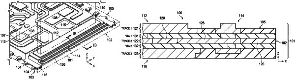
a multilayer lead frame having a first trace level, a second trace level, a via level, an insulator, a conductive landing pad and a conductive crack arrest structure, the first trace level including first patterned conductive features, the second trace level including second patterned conductive features, the via level including conductive vias that interconnect respective ones of the first and second patterned conductive features, the insulator extending between respective ones of the patterned conductive features and vias of the first trace level, the second trace level and the via level, the conductive landing pad disposed along a side of the multilayer lead frame, and a portion of the conductive crack arrest structure extending under a portion of the conductive landing pad;
an electronic component electrically coupled to the conductive landing pad; and
a package structure that encloses the electronic component and the conductive landing pad.
|