| CPC H01L 23/562 (2013.01) [H01L 23/585 (2013.01); H01L 25/0657 (2013.01); H01L 29/0657 (2013.01); H01L 2225/06541 (2013.01)] | 20 Claims |

|
1. A method of forming a semiconductor structure, comprising:
forming a group III-nitride (III-N) semiconductor material over a base silicon substrate at a first temperature;
cooling the group III-N semiconductor material and the base silicon substrate to a second temperature that is less than the first temperature, wherein cooling the group III-N semiconductor material and the base silicon substrate causes a plurality of cracks to form within a peripheral region of the group III-N semiconductor material, the peripheral region of the group III-N semiconductor material surrounding a central region of the group III-N semiconductor material; and
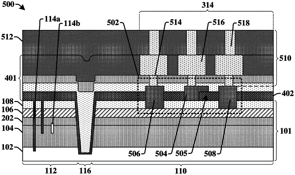
etching the group III-N semiconductor material and the base silicon substrate to form a crack stop ring trench that extends around the central region of the group III-N semiconductor material, wherein the crack stop ring trench separates the central region of the group III-N semiconductor material from the peripheral region of the group III-N semiconductor material.
|