| CPC H01L 23/562 (2013.01) [H01L 21/0223 (2013.01); H01L 21/3043 (2013.01); H01L 21/48 (2013.01); H01L 21/4853 (2013.01); H01L 21/4857 (2013.01); H01L 21/56 (2013.01); H01L 21/561 (2013.01); H01L 21/565 (2013.01); H01L 21/6835 (2013.01); H01L 21/78 (2013.01); H01L 23/3135 (2013.01); H01L 23/3178 (2013.01); H01L 23/3192 (2013.01); H01L 23/5383 (2013.01); H01L 23/5386 (2013.01); H01L 23/5389 (2013.01); H01L 24/18 (2013.01); H01L 21/486 (2013.01); H01L 21/568 (2013.01); H01L 23/3128 (2013.01); H01L 23/49816 (2013.01); H01L 23/5384 (2013.01); H01L 2221/6834 (2013.01); H01L 2221/68318 (2013.01); H01L 2221/68327 (2013.01); H01L 2221/68359 (2013.01); H01L 2221/68372 (2013.01); H01L 2221/68381 (2013.01); H01L 2224/118 (2013.01); H01L 2224/18 (2013.01)] | 20 Claims |
|
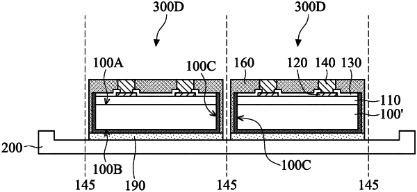
1. A package structure, comprising:
an adhesive layer;
a semiconductor substrate over the adhesive layer;
a dielectric layer on the semiconductor substrate;
a connector over the dielectric layer;
a first buffer layer surrounding the connector, the dielectric layer and the semiconductor substrate and covering the adhesive layer, wherein an interface between the adhesive layer and the first buffer layer is substantially level with a bottom surface of the semiconductor substrate;
a second buffer layer between the first buffer layer and the semiconductor substrate, wherein a topmost surface of the second buffer layer is substantially level with an interface between the dielectric layer and the semiconductor substrate;
an encapsulation layer surrounding the first buffer layer, wherein a bottommost surface of the first buffer layer is higher than a bottom surface of the encapsulation layer; and
a redistribution layer over the first buffer layer and the encapsulation layer.
|