| CPC H01L 23/562 (2013.01) [H01L 21/486 (2013.01); H01L 21/4853 (2013.01); H01L 21/4857 (2013.01); H01L 21/4871 (2013.01); H01L 21/563 (2013.01); H01L 21/565 (2013.01); H01L 21/568 (2013.01); H01L 21/6835 (2013.01); H01L 23/16 (2013.01); H01L 23/3128 (2013.01); H01L 23/3135 (2013.01); H01L 23/3675 (2013.01); H01L 23/5383 (2013.01); H01L 23/5384 (2013.01); H01L 23/5385 (2013.01); H01L 23/5386 (2013.01); H01L 23/585 (2013.01); H01L 2221/68372 (2013.01)] | 20 Claims |
|
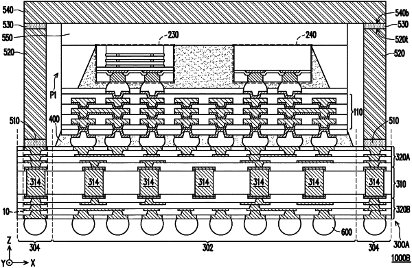
1. A package structure, comprising:
a circuit substrate, having a first region and a second region connected to and enclosing the first region, wherein a vertical projection of the first region is next to a vertical projection of the second region, wherein the circuit substrate comprises:
a core substrate;
a plurality of conductive vias, penetrating through the core substrate;
at least one routing layer, comprising a dielectric portion and a conductive portion disposed over the dielectric portion; and
at least one additional routing layer, wherein the at least one routing layer and the at least one additional routing layer are located on opposite sides of the core substrate and electrically coupled to each other through the plurality of conductive vias,
wherein a first ratio of a total volume of the conductive portion of the at least one routing layer within the first region to a total volume of the dielectric portion and the conductive portion of the at least one routing layer within the first region is less than a second ratio of a total volume of the conductive portion of the at least one routing layer within the second region to a total volume of the dielectric portion and the conductive portion of the at least one routing layer within the second region,
wherein a third ratio of a total volume of a conductive portion comprised in the core substrate within the first region to a total volume of a dielectric portion and a conductive portion comprised in the core substrate within the first region is less than a fourth ratio of a total volume of a conductive portion comprised in the core substrate within the second region to a total volume of a dielectric portion and a conductive portion comprised in the core substrate within the second region;
a semiconductor device, disposed over the circuit substrate within the first region, wherein the semiconductor device is electrically coupled to the circuit substrate; and
a ring structure, disposed over the circuit substrate within the second region.
|