| CPC H01L 23/5389 (2013.01) [H01L 21/4853 (2013.01); H01L 21/4857 (2013.01); H01L 21/4864 (2013.01); H01L 21/565 (2013.01); H01L 21/568 (2013.01); H01L 21/6835 (2013.01); H01L 23/3121 (2013.01); H01L 23/5383 (2013.01); H01L 23/5386 (2013.01); H01L 23/562 (2013.01); H01L 23/564 (2013.01); H01L 23/585 (2013.01); H01L 24/19 (2013.01); H01L 24/20 (2013.01); H01L 2221/68372 (2013.01); H01L 2224/214 (2013.01)] | 20 Claims |
|
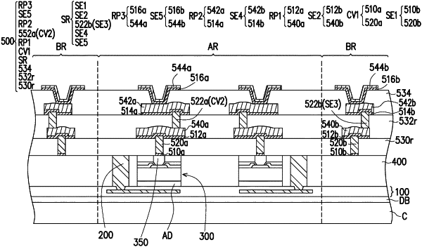
1. A package, comprising:
a die;
an encapsulant enclosing the die; and
a redistribution structure disposed on the die and located above the encapsulant, wherein the redistribution structure comprises:
a conductive via connected with the die;
a routing layer located above and connected with the conductive via;
a seal ring structure disposed on the encapsulant, wherein the seal ring structure comprises a first seal ring element, a second seal ring element, and a seed layer sandwiched between the first and second seal ring elements; and
a first dielectric layer and a second dielectric layer located above the first dielectric layer, wherein the first seal ring element and the conductive via are wrapped around by the first dielectric layer, the second seal ring element and the routing layer are wrapped around by the second dielectric layer, a top surface of the first seal ring element is substantially coplanar with a top surface of the conductive via.
|